- 您现在的位置:买卖IC网 > Sheet目录1998 > ICS843251BGI-15LF (IDT, Integrated Device Technology Inc)IC CLK GEN ETHERNET 25MHZ 8TSSOP
ICS843251I-15
FEMTOCLOCKCRYSTAL-TO-3.3V, 2.5V LVPECL CLOCK GENERATOR
IDT / ICS 3.3V, 2.5V LVPECL CLOCK GENERATOR
10
ICS843S51BGI-15 REV. A NOVEMBER 2, 2012
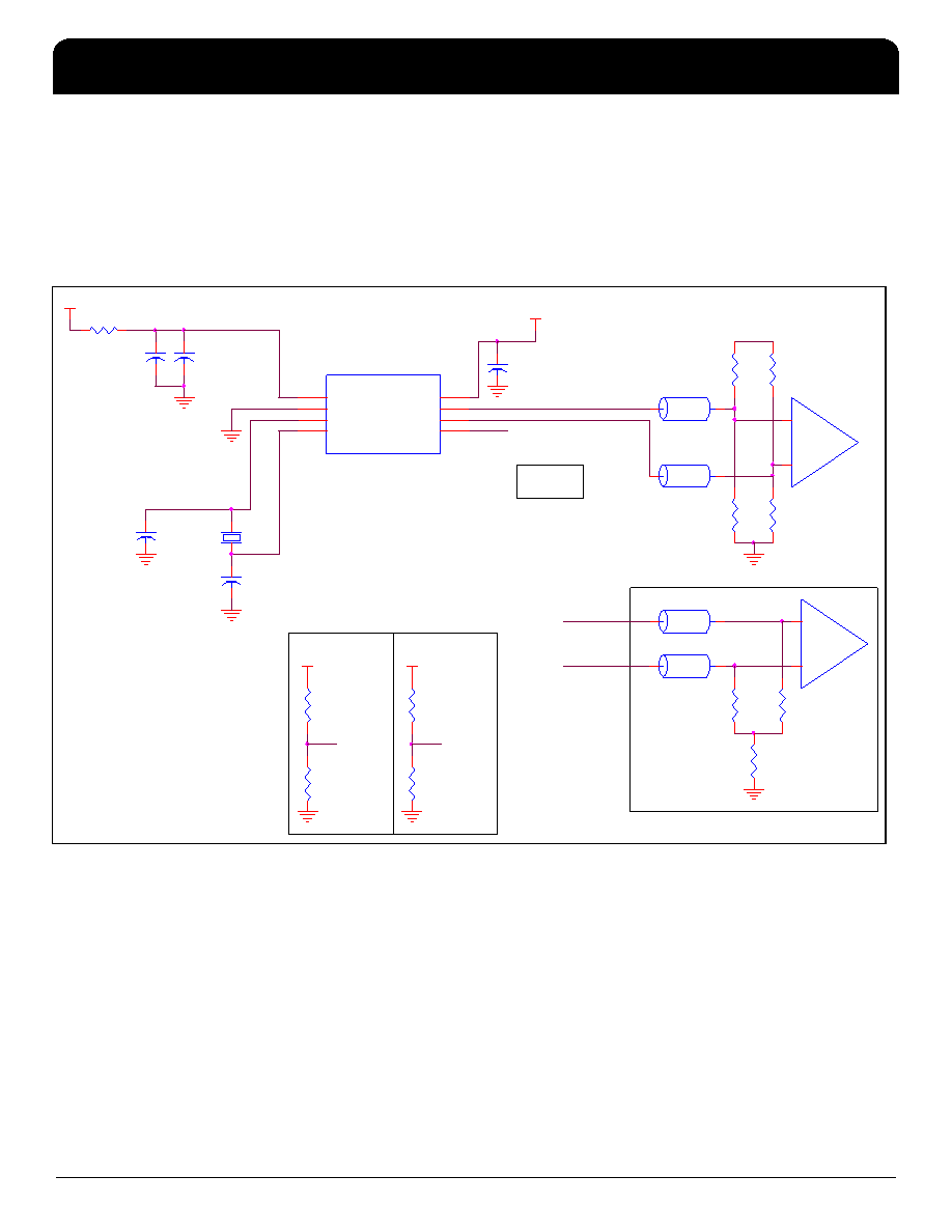
Schematic Example
Figure 6 shows an example of ICS843251I-15 application
schematic. In this example, the device is operated at VCC = 3.3V.
The 18pF parallel resonant 25MHz crystal is used. The C1 = 27pF
and C2 = 27pF are recommended for frequency accuracy. For
different board layout, the C1 and C2 may be slightly adjusted for
optimizing frequency accuracy. Two examples of LVPECL
termination are shown in this schematic. Additional termination
approaches are shown in the LVPECL Termination Application Note.
Note: Thermal pad (E-pad) must be connected to ground (VEE).
Figure 6. ICS843251I-15 Schematic Example
VCC
VCCA
C4
10uF
C5
0.01u
Zo = 50 Ohm
R3
133
To Logic
Input
pins
Zo = 50 Ohm
VCC
Set Logic
Input to
'0'
FREQ_SEL
VCC=3.3V
C1
27pF
C3
0.01u
1 8 p F
Q
Zo = 50 Ohm
RD1
Not Install
R1
10
XTAL_IN
R7
50
Optional
Y-Termination
To Logic
Input
pins
XTAL_OUT
3.3V
X1
25MHz
RD2
1K
VCC
U1
1
2
3
4
8
7
6
5
VCCA
VEE
XTAL_OUT
XTAL_IN
VCC
Q
nQ
FREQ_SEL
R2
133
Logic Control Input Examples
RU2
Not Install
R5
82.5
RU1
1K
nQ
C2
27pF
R4
82.5
R8
50
Zo = 50 Ohm
+
-
R6
50
Set Logic
Input to
'1'
+
-
发布紧急采购,3分钟左右您将得到回复。
相关PDF资料
ICS843253AGI-45LF
IC SYNTHESIZER LVPECL 16-TSSOP
ICS8432DY-101LFT
IC SYNTHESIZER 700MHZ 32-LQFP
ICS8432DYI-101LF
IC SYNTHESIZER 700MHZ 32-LQFP
ICS843SDNAGLF
IC GENERATOR FEMTOCLOCK 8TSSOP
ICS844001AGLFT
IC CLK GEN FIBRE CHAN 8-TSSOP
ICS844002AG-01LF
IC SYNTHESIZER 2LVDS 20-TSSOP
ICS844002AGI-01LFT
IC SYNTHESIZER 2LVDS 20-TSSOP
ICS844002AGLF
IC SYNTHESIZER 2LVDS 20-TSSOP
相关代理商/技术参数
ICS843251BGI-15LFT
功能描述:IC CLK GEN ETHERNET 25MHZ 8TSSOP RoHS:是 类别:集成电路 (IC) >> 时钟/计时 - 时钟发生器,PLL,频率合成器 系列:HiPerClockS™, FemtoClock™ 标准包装:1,000 系列:- 类型:时钟/频率合成器,扇出分配 PLL:- 输入:- 输出:- 电路数:- 比率 - 输入:输出:- 差分 - 输入:输出:- 频率 - 最大:- 除法器/乘法器:- 电源电压:- 工作温度:- 安装类型:表面贴装 封装/外壳:56-VFQFN 裸露焊盘 供应商设备封装:56-VFQFP-EP(8x8) 包装:带卷 (TR) 其它名称:844S012AKI-01LFT
ICS843251BGI-15T
制造商:Integrated Device Technology Inc 功能描述:IC SYNTHESIZER LVPECL 8TSSOP
ICS843251I-12
制造商:ICS 制造商全称:ICS 功能描述:FEMTOCLOCKS? CRYSTAL-TO-3.3V, 2.5V LVPECL CLOCK GENERATOR
ICS8432-51K
制造商:ICS 制造商全称:ICS 功能描述:700MHZ, CRYSTAL-TO-3.3V DIFFERENTIAL LVPECL FREQUENCY SYNTHESIZER
ICS843252
制造商:ICS 制造商全称:ICS 功能描述:FEMTOCLOCKS⑩ CRYSTAL-TO-3.3V LVPECL FREQUENCY SYNTHESIZER
ICS843252-04
制造商:ICS 制造商全称:ICS 功能描述:FEMTOCLOCKS⑩ CRYSTAL-TO-3.3V LVPECL CLOCK GENERATOR
ICS843252AG
制造商:ICS 制造商全称:ICS 功能描述:FEMTOCLOCKS⑩ CRYSTAL-TO-3.3V LVPECL FREQUENCY SYNTHESIZER
ICS843252AG-04
制造商:ICS 制造商全称:ICS 功能描述:FEMTOCLOCKS? CRYSTAL-TO-3.3V LVPECL CLOCK GENERATOR